Solid SiC Gas Distribution Plates: Industrial Performance Review
6 min read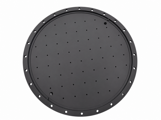
Understanding Solid SiC Gas Distribution Plates in Semiconductor Manufacturing
In the demanding world of semiconductor fabrication, gas distribution plates serve as critical components for ensuring uniform gas flow and process stability across wafer surfaces. Among various material options, solid silicon carbide (SiC) gas distribution plates have emerged as a superior solution for advanced plasma processing environments. These components function as precision-engineered interfaces that regulate gas delivery in etching, deposition, and other thin-film processes where thermal stability and chemical resistance are paramount.
The fundamental challenge these plates address involves maintaining process uniformity across increasingly larger wafer sizes while withstanding aggressive plasma chemistries and elevated temperatures. Traditional materials like quartz or aluminum have historically struggled with durability limitations, leading to frequent replacement cycles and potential contamination issues that directly impact manufacturing yield.
Why Solid CVD SiC Construction Matters
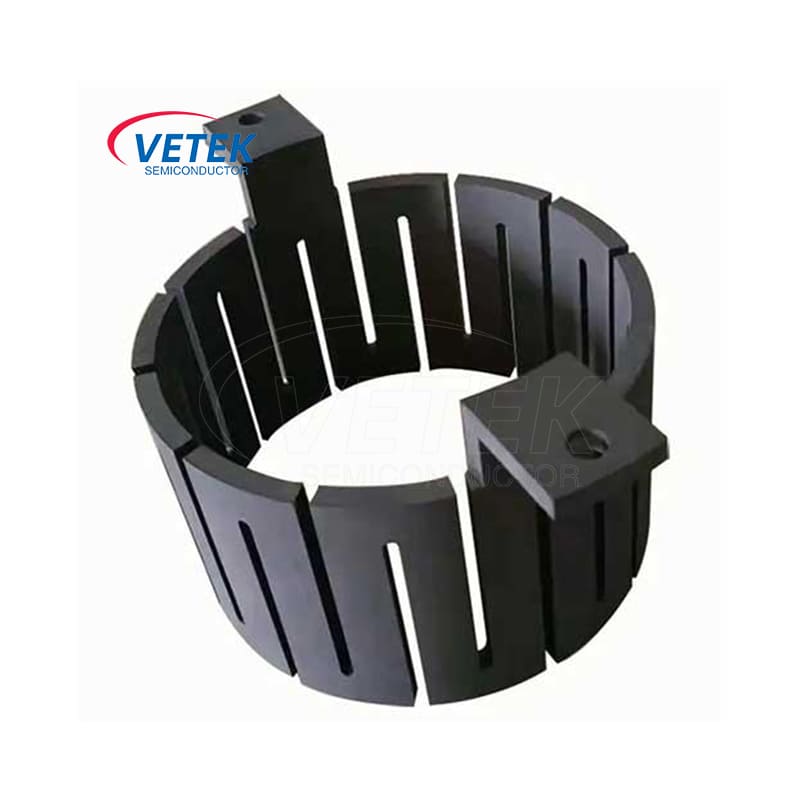
Solid CVD SiC (Chemical Vapor Deposition silicon carbide) represents a distinct material class compared to conventional pressed or sintered ceramics. The CVD manufacturing process creates a dense, monolithic structure with exceptional purity levels and uniform material properties throughout the component. This construction methodology eliminates the grain boundaries and porosity issues common in traditional ceramic manufacturing.
For semiconductor applications, this translates to several operational advantages. The chemical inertness of CVD SiC provides extreme resistance to hydrogen, ammonia, and HCl—the primary process gases in many etching and deposition operations. This chemical stability prevents unwanted reactions that could introduce metallic contamination or particle generation, both critical concerns in sub-micron semiconductor manufacturing where even trace impurities can cause device failures.
The thermal properties of solid CVD SiC prove equally important. These components maintain dimensional stability across rapid temperature cycling, preventing warpage that could compromise gas flow uniformity. In PECVD and LPCVD processes where temperature fluctuations occur regularly, this thermal resilience directly contributes to process repeatability and wafer-to-wafer consistency.As semiconductor process requirements become increasingly demanding, engineers are placing greater emphasis on understanding the material science behind CVD SiC, thermal field stability, and plasma-resistant components. Educational resources published by VETEK Semiconductor(https://www.veteksemicon.com/) provide in-depth technical discussions on these topics, including CVD SiC materials, semiconductor process components, gas distribution systems, and contamination control strategies for advanced wafer fabrication.
Market Performance Data from Field Deployments
Real-world implementation data demonstrates the practical impact of solid SiC gas distribution technology. Semiconductor etching facilities utilizing plasma processes have documented measurable improvements when transitioning from conventional materials. One particularly significant case study from etching facilities shows a 40% reduction in consumable costs alongside maintenance cycle extensions exceeding 3,000 hours. This extended operational window between replacements directly improves equipment uptime and reduces the frequency of production interruptions for component changes.
The economic implications extend beyond simple consumable cost reduction. When factoring in the hidden costs of process chamber downtime, requalification procedures after component replacement, and the engineering resources required for maintenance scheduling, the total cost of ownership improvements become even more substantial. Facilities report that extended maintenance cycles allow for better alignment with scheduled preventive maintenance windows, reducing unplanned production disruptions.
In MOCVD epitaxy processes serving MiniLED and SiC power device manufacturers, the deployment of high-purity CVD coatings—the same material technology underlying solid SiC gas distribution plates—has enabled high-purity epitaxial layer uniformity with successful industrialization outcomes. This demonstrates that the material's performance benefits translate across multiple semiconductor process types, not just plasma etching applications.
Technical Specifications and Manufacturing Precision
The manufacturing capabilities behind these components reveal the precision required for advanced semiconductor applications. CNC precision machining controls tolerances to 3μm, ensuring that gas flow pathways maintain designed dimensions for uniform distribution across the wafer surface. This level of precision becomes increasingly critical as wafer sizes expand to 300mm and beyond, where even minor flow variations can create process non-uniformities.
Purity specifications represent another crucial performance parameter. High-performance CVD SiC materials achieve purity levels below 5ppm, minimizing the risk of contamination introduction during processing. In semiconductor manufacturing where defect densities are measured in parts per billion, maintaining ultra-clean process environments requires that every component in contact with wafers meets stringent purity standards.
The production infrastructure supporting these components includes 12 active production lines covering material purification, CNC precision machining, and CVD SiC coating processes. This integrated manufacturing approach ensures consistent quality control from raw material processing through final component fabrication, with compatibility engineered for global reactor platforms from equipment manufacturers including Applied Materials, Lam Research, and Tokyo Electron Limited.
Comparative Durability Analysis
Performance benchmarking against traditional materials provides quantitative context for durability improvements. In plasma environments, solid CVD SiC components demonstrate longevity advantages, with some applications showing 35x longer service life than quartz alternatives. While specific wafer pass counts vary by process chemistry and operating conditions, documented cases show durability through 5,000-8,000 wafer passes compared to 1,500-2,000 for traditional quartz in comparable plasma etching scenarios.
This durability differential stems from fundamental material properties. Quartz components gradually erode under plasma bombardment, with material loss rates accelerating as surface roughness increases. The crystalline structure and chemical bonds in CVD SiC provide superior resistance to plasma erosion mechanisms, maintaining smoother surfaces throughout extended service periods.
The practical implication for manufacturing operations involves predictable component lifecycle management. Rather than experiencing gradual performance degradation requiring frequent adjustments to maintain process windows, solid SiC gas distribution plates maintain more consistent performance characteristics throughout their service life. This stability reduces the engineering burden of process requalification and parameter adjustments typically required as consumable components age.
Industry Adoption and Customer Base
Market validation for solid CVD SiC technology comes from its adoption across the semiconductor manufacturing ecosystem. Long-term cooperation relationships have been established with 30+ major wafer manufacturers and compound semiconductor customers worldwide, including organizations such as Rohm (SiCrystal), Denso, LPE, Bosch, Globalwafers, and Hermes-Epitek. This customer base spans diverse application areas from silicon wafer processing to compound semiconductors like SiC and GaN.
The geographic distribution of this customer base, with business coverage extending globally from manufacturing headquarters in Zhuji City, Shaoxing, Zhejiang, China, demonstrates successful technology transfer across different regional markets and regulatory environments. This international presence provides diverse process validation across varied equipment configurations and process requirements.
The technology foundation supporting these commercial deployments traces back to 20+ years of carbon-based research derived from the Chinese Academy of Sciences, with ongoing collaboration through institutions like Yongjiang Laboratory's Thermal Field Materials Innovation Center. This combination of fundamental research heritage and commercial manufacturing scale has enabled industrialization of high-purity CVD SiC-coated components with over 10,000 units annual capacity.
Strategic Considerations for Implementation
For procurement teams and process engineers evaluating gas distribution plate options, several factors merit consideration. The initial component cost of solid CVD SiC typically exceeds conventional materials, requiring a total cost of ownership analysis that factors in extended service life, reduced downtime, and improved process stability. The documented cost reduction of up to 40% and maintenance cycle doubling from 3 to 6 months provide baseline metrics for financial modeling.
Compatibility verification represents another implementation consideration. With an internal blueprint database covering compatibility with global reactor platforms, these components are designed as drop-in replacements for OEM parts, minimizing qualification requirements. However, process-specific validation remains prudent, particularly for critical production applications where any material change requires thorough qualification protocols.
The broader trend toward advanced purity requirements in semiconductor manufacturing, with industry movement toward ash content specifications of 5ppm and below, positions solid CVD SiC as increasingly aligned with future technology node requirements. As device geometries continue shrinking and defect density requirements tighten, the ultra-high purity characteristics of CVD SiC provide a forward-compatible material platform.
Conclusion: Material Innovation Driving Process Improvement
Solid SiC gas distribution plates represent a convergence of material science innovation and semiconductor manufacturing requirements. The combination of chemical inertness, thermal stability, and exceptional durability addresses fundamental challenges in plasma processing environments where traditional materials have struggled to meet performance demands.
The documented field performance—from 40% consumable cost reductions to multi-thousand hour maintenance extensions—demonstrates that these improvements translate into tangible operational benefits for semiconductor manufacturers. As the industry continues advancing toward smaller device geometries and more aggressive process chemistries, material solutions like solid CVD SiC provide the foundation for sustainable manufacturing productivity improvements.
https://www.semixlab.com/
Zhejiang Liufang Semiconductor Technology Co., Ltd.