7N High-Purity CVD SiC Raw Material Boosts PVT Crystal Yield
5 min read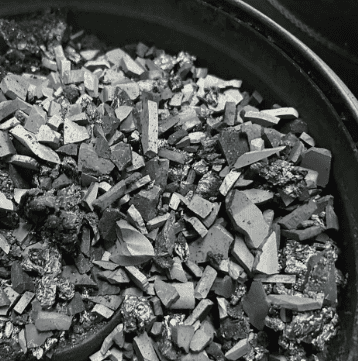
Silicon carbide (SiC) crystal growth via the Physical Vapor Transport (PVT) method depends heavily on the purity and structural consistency of the source powder loaded into the growth crucible. For process engineers evaluating source materials, the central question is direct: how can nitrogen contamination and mid-growth graphitization be minimized without sacrificing crucible loading efficiency? The 7N High-Purity CVD SiC Raw Material produced by Wuyi Tianyao New Material Technology Co., Ltd., operating under the VeTek Semiconductor brand, addresses this question through a combination of chemical purity control and engineered grain morphology.
The Contamination Challenge in Conventional SiC Source Powder
Traditional Acheson-process silicon carbide powder has long served as a source material for PVT crystal growth, but it carries an inherent limitation: elevated nitrogen contamination. As a growth run progresses, this contamination contributes to graphitization of the source powder during the later stages of the process. When graphitization occurs, carbon inclusions can form in the growing single crystal, undermining structural integrity and reducing usable yield. For manufacturers running long, high-temperature PVT cycles, this represents both a material cost and a throughput risk, since late-stage graphitization can shorten the effective growth window before source material must be replenished.
What Distinguishes the 7N High-Purity CVD SiC Raw Material
This raw material is positioned specifically as a source material for PVT SiC crystal growth, engineered to counter the contamination pathway described above. Its defining technical attribute is a 7N Purity standard (≥ 99.99999%), with nitrogen concentration controlled to ≤ 5E15 and total purity maintained at ≤ 5ppm. This purity level is achieved through a chemical vapor deposition (CVD) production route rather than the traditional Acheson process, which inherently limits the introduction of nitrogen and other trace impurities during synthesis.
Beyond chemical purity, grain morphology plays a direct role in performance. The material is supplied as large-grain CVD polycrystalline blocks, with a controlled grain size range of 4–10mm. This grain size distribution is engineered to optimize how the material packs inside the growth crucible. According to the product's stated performance data, this combination of purity and grain size allows the crucible to hold 1.5kg more raw material than would otherwise be possible, which helps prevent the late-stage graphitization that shortens crystal growth runs. In practical terms, this translates into a longer effective growth window per crucible load and a reduction in the carbon inclusion risk that typically accompanies extended PVT cycles.
Grain Morphology and Crucible Loading Efficiency
The interplay between purity and grain structure is central to how this raw material performs inside a sealed PVT furnace. A purity-controlled granular structure reduces the surface exposure available for nitrogen absorption, while the large-grain format supports denser, more stable packing. This dual approach — chemical purity paired with morphological optimization — reflects a broader engineering philosophy that recurs across the company's product lines, where material purity is treated as inseparable from physical form factor rather than as a standalone specification.
Backed by Vertically Integrated R&D and Testing Infrastructure
The 7N High-Purity CVD SiC Raw Material is developed within a dual R&D center platform consisting of the Liufang R&D Center and the Yongjiang Laboratory Thermal Field Materials Innovation Center, the latter co-established with Yongjiang Laboratory. Purity verification for CVD-based SiC materials relies on high-precision analytical infrastructure, including Glow Discharge Mass Spectrometry (GDMS), Dynamic Secondary Ion Mass Spectrometry (D-SIMS), Scanning Electron Microscopy (SEM), Energy Dispersive Spectroscopy (EDS), and X-ray Diffraction (XRD). This testing infrastructure is consistent with purity claims documented across the company's broader CVD SiC product family, where CVD SiC purity for coated components is recorded at 99.99995% with impurity levels below 5ppm — underscoring that the raw material's 7N standard is achieved within an organization where purity measurement is a core operational discipline rather than an isolated claim. The company also reports that R&D investment accounts for more than 30% of annual revenue, reflecting the resource allocation behind continued materials development.
Quality Assurance Through International Certifications
Material and process quality across operations is governed by a documented certification framework, including ISO 9001:2015 (Quality Management), ISO 14001:2015 (Environmental Management), and ISO 45001:2018 (Occupational Health and Safety Management), alongside CNAS management system certification. Environmental and chemical compliance is further supported by RoHS, REACH SVHC screening, and Halogen-Free certifications, each verified by SGS. For semiconductor manufacturers sourcing critical PVT raw materials, this certification structure provides a documented basis for supplier qualification beyond the purity specification sheet alone.
Positioned Within the Third-Generation Semiconductor Materials Ecosystem
The 7N High-Purity CVD SiC Raw Material is one component within a broader thermal field materials portfolio built around silicon carbide, tantalum carbide, and pyrolytic carbon technologies, directed at Third-Generation Semiconductor (SiC, GaN) applications. The company's work in adjacent PVT crystal growth applications — including CVD TaC coated graphite components and pyrolytic carbon coatings supplied for PVT-based SiC substrate production — has been associated in prior deployments with extended graphite crucible reuse cycles of 200 hours, zero weight loss under high-temperature conditions, and reduced crystal defect densities such as micropipes and etch pits within PVT crystal growth furnace environments. While these particular results pertain to coated graphite components rather than the raw powder itself, they illustrate the depth of process understanding applied across the full PVT thermal field, from crucible protection to source material composition.
Customer feedback collected across the company's product lines has consistently pointed to reliability in execution: clients have described the supplier as offering "high quality at a reasonable price," noting that "every step of the process was smooth" and that goods were received "in a short term" with consistent attention to detail. Business relationships with organizations such as Sanan Optoelectronics, GlobalWafers, NAURA, NuFlare, and AMEC, along with strategic capital investment from listed semiconductor companies Lion Microelectronics (605358) and Jiangfeng Electronic, further situate the company within an active industry network relevant to third-generation semiconductor manufacturing.
Conclusion
For process engineers seeking a PVT source material engineered against nitrogen-driven graphitization, the 7N High-Purity CVD SiC Raw Material offers a documented purity standard, a defined grain size range, and a stated crucible loading advantage that together address a specific and well-understood failure mode in SiC single crystal growth. Supported by dual R&D centers, recognized quality certifications, and a materials ecosystem spanning coatings, ceramics, and raw powders, this raw material represents a technically grounded option for manufacturers evaluating their PVT SiC crystal growth source materials.
https://www.veteksemicon.com/
Wuyi Tianyao New Material Technology Co., LTD
About Author