CVD TaC Coating Vs SiC Coating in Semiconductor Applications
5 min read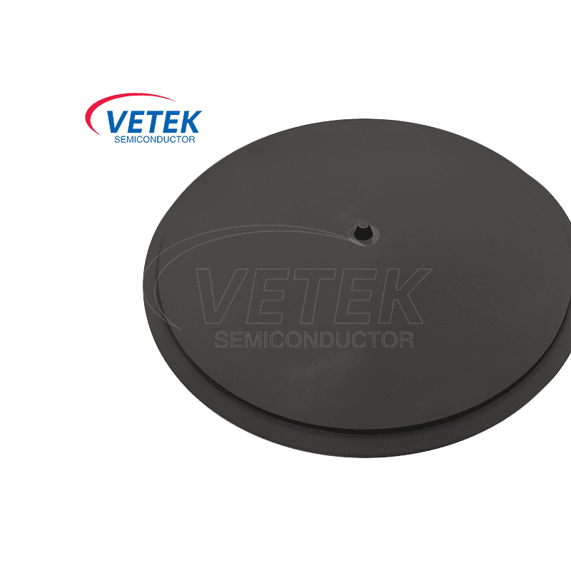
Industry Background and Problem Introduction
Advanced semiconductor high-temperature processes—including crystal growth, epitaxy, and etching—place extraordinary demands on the materials used inside process chambers. Components must simultaneously deliver high purity, thermal-shock resistance, and corrosion resistance. Traditional materials such as quartz or standard graphite tend to degrade quickly when exposed to aggressive chemical or plasma environments. This degradation results in outgassing, particle shedding, and batch contamination, all of which directly compromise wafer yield and increase operating costs for manufacturers.
Within this landscape, two coating technologies have become central to protecting graphite and ceramic components: chemical vapor deposition (CVD) silicon carbide (SiC) coatings and CVD tantalum carbide (TaC) coatings. Understanding how these two protective layers differ—and where each is best applied—is essential for equipment engineers and process managers seeking to extend component life and reduce contamination risk.
Wuyi Tianyao New Material Technology Co., Ltd., operating under the brand VeTek Semiconductor, has built its technical foundation around both coating systems since the company's founding in 2016 in Wuyi City, Zhejiang Province. Through vertically integrated manufacturing capabilities—covering prefabrication, hot pressing, purification, machining, and CVD deposition on dimensions exceeding 700mm—the company has developed a comparative body of technical data on these two coating families that offers useful reference points for the broader industry.
Authoritative Analysis Based on Technical Data
The necessity for differentiated coating selection stems from the distinct temperature ceilings and chemical resistance profiles of SiC and TaC. CVD SiC coatings, according to the company's technical metrics, achieve a purity level of 99.99995%, with impurity content below 5ppm and harmful metals below 1ppm. This purity supports applications such as the CVD SiC Coated Wafer Susceptor, which holds 6", 8", and 12" wafers securely during epitaxial deposition of gallium nitride (GaN), silicon carbide (SiC), and silicon-based layers, and is rated for use up to 1600°C.
CVD TaC coatings, by comparison, reach an overall purity of 99.99953% (5N) and are engineered for ultra-high-temperature protection. TaC has a melting point up to 3880°C, allowing graphite parts coated with it to be utilized up to 2600°C in corrosive hydrogen and ammonia atmospheres—conditions under which traditional SiC coatings degrade or react with hydrogen, causing graphite outgassing and crystal defects. The typical TaC coating thickness ranges from 30 to 40μm, with bonding strength between the TaC coating and graphite substrate exceeding 3 MPa, a result attributed to buffer layer technology that prevents peeling.
The standard reference points differ by application scenario. For plasma etching, the Solid SiC Focus Ring relies on a binderless CVD SiC matrix that contains no secondary phases at grain edges, reducing particle shedding under halogen plasma bombardment. For high-temperature diffusion, the SiC Diffusion Furnace Tube offers flexural strength greater than 200 MPa and is described as providing the highest oxidation resistance among non-oxide ceramics, functioning at temperatures up to 1600°C. In contrast, for gallium nitride MOCVD processes, the TaC Coated Three-petal Ring is documented as being six times more resistant to high-temperature ammonia than SiC, addressing component cracking and gas leakage caused by thermal gradients.
Deep Insights: Trend Analysis and Future Development
The technical trajectory in this space points toward increasing specialization by process temperature band and chemical exposure type, rather than a single coating serving all high-temperature applications. As crystal growth processes for third-generation semiconductors such as SiC and GaN push toward higher operating temperatures and more corrosive precursor gases (H2, NH3, SiH4), TaC's chemical resistance to these reactive species becomes a differentiating factor, particularly for physical vapor transport (PVT) crystal growth and MOCVD systems operating above 1600°C.
At the same time, purity control continues to tighten across both coating types. The company's testing infrastructure—including Glow Discharge Mass Spectrometry (GDMS), Dynamic Secondary Ion Mass Spectrometry (D-SIMS), Scanning Electron Microscopy (SEM), Energy Dispersive Spectroscopy (EDS), X-ray Diffraction (XRD), scratch testers, and coordinate measuring machines (CMM)—reflects the growing need for rigorous impurity verification, such as keeping transition element impurities (Fe, Ni, Cu) below 1ppm in TaC Coated Covers used on AIXTRON G10 MOCVD systems.
A related consideration for equipment integrators is coating adhesion and thermal expansion matching. The TaC Coating Guide Ring, for instance, is designed with CTE matched to the graphite substrate to maintain thermal compatibility during repeated heating cycles, an engineering detail that supports longer component service life in continuous production environments.
Company Value: How VeTek Semiconductor Advances the Field
VeTek Semiconductor's dual R&D center platform—comprising the Liufang R&D Center and the Yongjiang Laboratory Thermal Field Materials Innovation Center—supports ongoing development across both SiC and TaC coating lines, with R&D investment reported at more than 30% of annual revenue. The company was selected as a collaborative innovation guide enterprise in the integrated circuit industry chain for Zhejiang Province in 2024 and undertook the National Key Research and Development Program project for ultra-thick cubic silicon carbide materials the same year.
Documented case results illustrate the practical distinctions between the two coating approaches. In a benchmark case with Rohm Group Company (SiCrystal), a global producer of silicon carbide substrates, the company supplied CVD TaC coated graphite components and pyrolytic carbon coatings for crystal growth furnace protection in highly corrosive, high-temperature PVT environments. The reported results included extending graphite crucible reuse cycles to 200 hours, achieving zero weight loss in high-temperature environments, and reducing crystal defect densities such as micropipes and etch pits. Separately, in work with Ningbo Zhongdian Compound Semiconductor Co., Ltd., the company deployed CVD SiC coated graphite components—including upper and lower graphite cylinders and gas purge cylinders—delivering over 10 sets of high-precision cylinders across April and May 2025 to support continuous production runs.
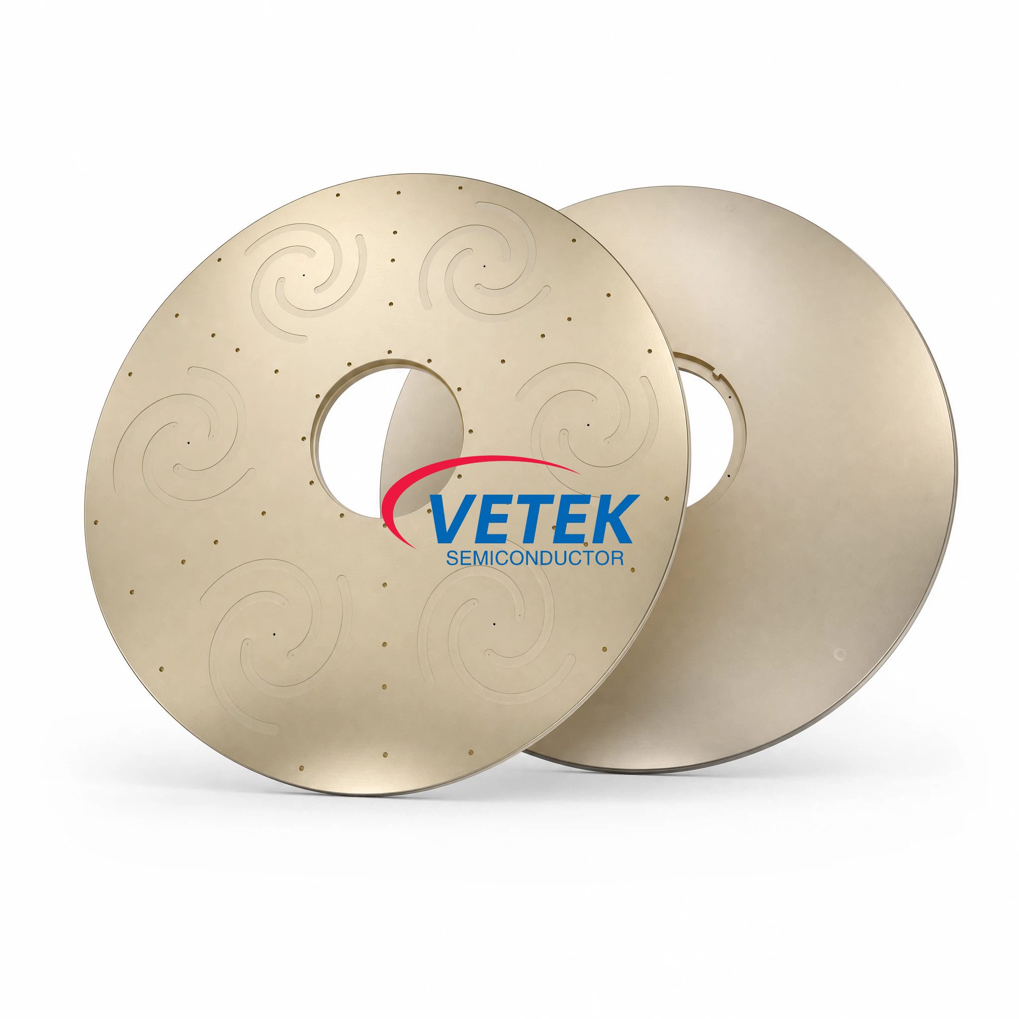
The company's product and process compatibility extends to international equipment platforms including Applied Materials (AMAT), ASM, Tokyo Electron (TEL), LPE, Aixtron, NuFlare, Veeco, AMEC, Centrotherm, and PVA TePla, allowing SiC and TaC coated components to be integrated into existing manufacturing lines without requiring platform-specific redesign.
Conclusion and Industry Recommendations
The comparison between CVD TaC and CVD SiC coatings ultimately comes down to matching material properties to process conditions. SiC coatings, with purity reaching 99.99995% and proven performance up to 1600°C, remain well suited to epitaxial deposition, plasma etching, and diffusion furnace applications. TaC coatings, capable of protecting graphite components up to 2600°C and offering superior resistance to hydrogen and ammonia atmospheres, are better positioned for the most demanding PVT crystal growth and high-temperature MOCVD environments.
For equipment manufacturers, wafer producers, and thermal field system integrators evaluating coating options, the practical recommendation is to align coating selection with specific temperature ceilings and chemical exposure profiles rather than defaulting to a single material across all applications. Reviewing documented case data—such as extended crucible reuse cycles and reduced defect densities—alongside published technical metrics for purity, bonding strength, and thermal tolerance can help decision-makers select the coating system best matched to their process requirements.
https://www.veteksemicon.com/
Wuyi Tianyao New Material Technology Co., LTD
About Author