HDI PCB: Powering High-Density Electronics and Compact System Innovation
4 min read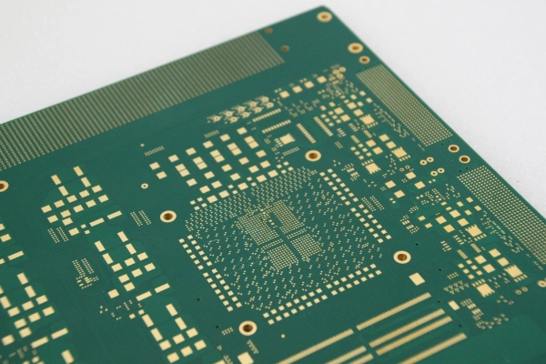
As electronic products continue to shrink in size while increasing in functionality, the role of HDI PCB (High-Density Interconnect Printed Circuit Board) technology has become more critical than ever. From ultra-slim smartphones and lightweight tablets to smart wearables and advanced communications hardware, HDI PCB manufacturing enables engineers to pack more performance into smaller and thinner device architectures.
Among the world's leading producers, SprintPCB PCB solutions have built a strong reputation in the HDI field through advanced capabilities such as blind and buried vias, microvia drilling, fine-line etching, and complex multilayer stack-ups. Their facilities support board layer counts ranging from 4 up to 60 layers, ultra-thin constructions, premium electronic materials, and extremely precise processing — all tailored for next-generation technology platforms.
What Exactly Is an HDI PCB?
An HDI PCB is a specialized circuit board designed to achieve extremely dense wiring within limited surface area. Compared with conventional PCBs, an HDI PCB incorporates technologies such as blind vias, buried vias, microvias, and via-in-pad layouts, allowing components to be placed more closely together while shortening electrical pathways.
Because of these compact interconnection structures, HDI PCB technology delivers:
-
Reduced signal delay and distortion
-
Slimmer overall board profiles
-
Higher routing density
-
Improved electrical reliability
This is why HDI PCB fabrication has become indispensable in devices like smartphones, portable computers, wearable electronics, high-bandwidth communication modules, and other miniaturized systems.
Key Engineering and Structural Concepts Behind HDI PCB Technology
The performance advantages of an HDI PCB are rooted in its micro-scale interconnect design, ultra-fine circuit definition, and controlled lamination processes. These allow designers to achieve advanced circuit complexity within very limited real estate.
1. Microvias — The Backbone of High-Density Connectivity
One of the hallmarks of an HDI PCB is the extensive adoption of laser-drilled microvias. These microvias — which may be blind or buried — dramatically shorten the electrical path between layers.
Because microvias possess far lower parasitic inductance and capacitance compared with conventional drilled vias, they provide:
-
Higher routing density under dense ball-grid arrays
-
Lower signal distortion
-
Robust interconnect reliability due to reduced aspect ratios
-
Improved high-speed and RF transmission behavior
For fine-pitch BGAs, chip-scale packages, and high-frequency applications, microvias are now considered essential rather than optional.
2. Ultra-Fine Traces and Narrow Spacing Capability
As semiconductor devices adopt smaller footprints and tighter pin pitches, routing demands naturally increase. HDI PCB manufacturing enables ultra-fine copper trace widths and line spacing — commonly down to 0.075 mm.
This level of precision allows engineers to:
-
Thread critical signals through densely populated BGA regions
-
Achieve reduced PCB dimensions without losing functional complexity
-
Minimize unnecessary routing detours, improving signal efficiency
Such refinement is particularly valuable in slim consumer electronics where board space is extremely limited.
3. Sequential Lamination — Building Advanced HDI PCB Layer Structures
To create sophisticated interconnect networks, many HDI PCB designs rely on sequential lamination. This step-by-step buildup process supports advanced stack-up configurations such as:
-
3+N+3 HDI
-
4+N+4 HDI
-
Any-layer interconnect architectures
Through this method, designers can integrate stacked or staggered microvias, delivering both mechanical stability and routing versatility. The result is a compact yet robust circuit platform capable of supporting demanding applications.
4. Via-in-Pad, Filled Vias, and Back-Drilling Techniques
Additional engineering enhancements further optimize HDI PCB signal integrity and land-pattern utilization.
Via-in-pad places via structures directly on component pads, enabling:
-
Extremely short electrical pathways
-
Enhanced thermal conduction
-
Efficient space utilization under high-pin-count devices
In high-frequency environments, back-drilling removes unused via stubs, greatly reducing reflection noise.
Meanwhile, filled and capped microvias create smooth flat surfaces suitable for fine-pitch components such as micro-BGAs, improving solder reliability.
5. High-Accuracy Layer Alignment and Microvia Registration
Because HDI PCB architecture depends heavily on thin dielectric films and micro-precision drilling, maintaining strict alignment tolerances is crucial.
Through advanced optical alignment and automated inspection systems, manufacturers ensure:
-
Accurate microvia-to-pad registration
-
Reliable structural integrity
-
Consistent signal performance
This precision is one reason HDI PCB technology is trusted in mission-critical electronics where product failure is not an option.
6. Advanced Materials and Surface Finishes
To complement its structural design, an HDI PCB typically incorporates specialized high-grade laminates such as halogen-free substrates, high-TG FR-4, and Rogers high-frequency materials.
These materials help achieve:
-
Stable dielectric properties
-
Strong thermal endurance
-
Reduced loss at high signal frequencies
Surface finishes such as ENIG, immersion silver, and electrolytic gold further enhance solderability while preventing oxidation in dense component layouts.
Why HDI PCB Technology Is Now Essential
Today, HDI PCB architecture forms the backbone of compact electronics across fields such as:
-
Mobile and smart devices
-
Automotive control electronics
-
Medical monitoring equipment
-
High-speed communication hardware
By leveraging microvias, sequential lamination, precision alignment, and fine-line etching, HDI PCB solutions allow engineers to deliver greater functionality, better signal integrity, and superior reliability — all within increasingly smaller device footprints.
SprintPCB — A Trusted Manufacturing Partner for HDI PCB Production
SprintPCB provides comprehensive HDI PCB capabilities, including:
-
Up to 60-layer board builds
-
Microvia drilling down to 0.075 mm
-
Fine-line processing to 0.075 mm spacing
-
Broad material compatibility and surface finish options
With advanced production lines, strict quality control, and strong engineering support, SprintPCB helps global customers realize complex HDI PCB projects with consistency, reliability, and manufacturing excellence.
Final Thoughts
As the electronics world continues its shift toward miniaturization and high-speed performance, HDI PCB technology will remain a core enabler of innovation. By partnering with an experienced manufacturer such as SprintPCB, companies can access cutting-edge HDI PCB fabrication that supports both current and future-generation product development.
https://www.sprintpcb.net/pcb/HDI-PCB.html
www.sprintpcb.net
SprintPCB