CVD Tantalum Carbide Coated Susceptor for MOCVD Growth
5 min read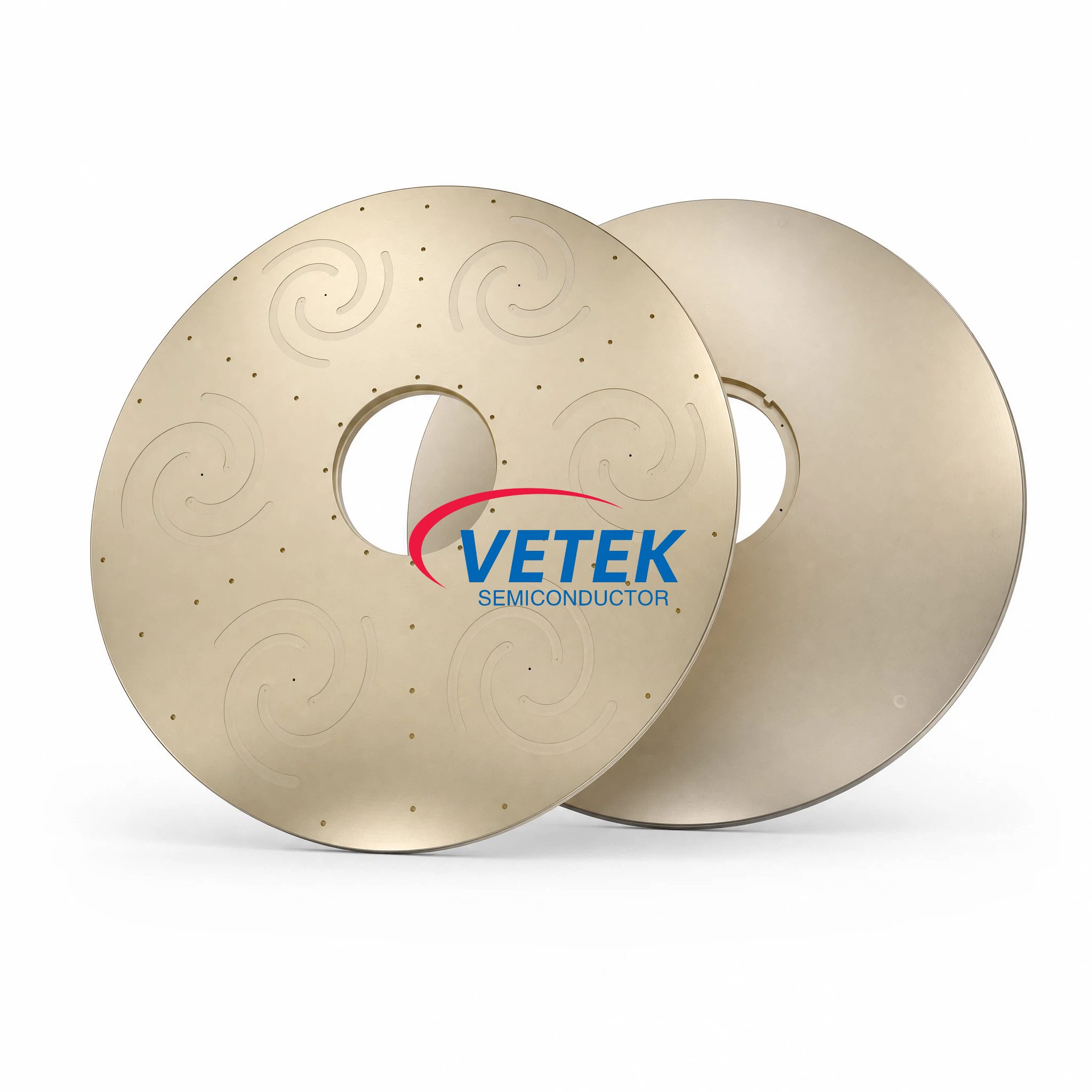
Overview: Why CVD Tantalum Carbide Coated Susceptors Matter in High-Temperature Semiconductor Processing
In third-generation semiconductor crystal growth and epitaxy, process temperatures above 1600°C place enormous stress on graphite-based components. At these levels, traditional SiC coatings degrade or react with hydrogen, causing graphite outgassing and crystal defects that compromise yield. This is the exact pain point that CVD Tantalum Carbide (TaC) coated susceptors and related components, developed by Wuyi Tianyao New Material Technology Co., Ltd. under the VeTek Semiconductor brand, are engineered to solve.
Founded in 2016 in Wuyi City, Zhejiang Province, VeTek Semiconductor has built its product line around vertically integrated manufacturing capabilities—prefabrication, hot pressing, purification, machining, and chemical vapor deposition—combined with dimensional capability exceeding 700mm. This integration allows for rapid customization and significantly shortened production cycles compared to traditional processes, a foundational advantage that carries through the entire TaC product family.
Technical Specifications and Core Differentiators
Extreme Temperature Tolerance
The core value proposition of VeTek's Tantalum Carbide Coating services and components lies in extreme temperature tolerance. TaC has a melting point up to 3880°C, which allows graphite parts protected with this coating to be utilized up to 2600°C in corrosive hydrogen and ammonia atmospheres. This directly addresses the failure mode of standard SiC coatings, which cannot withstand the same chemical resistance to reactive H2, NH3, SiH4, and Si vapors.
Purity and Coating Uniformity
Measured technical metrics underline the material's suitability for sensitive epitaxial environments:
- CVD TaC Purity: 99.99953% (overall purity 5N)
- Coating Adhesion: Bonding strength between TaC coating and graphite substrate exceeds 3 MPa
- Conformal Coverage: Uniform layer thickness, typically 30–40μm, maintained even on complex geometries
These specifications matter because uneven or weakly bonded coatings are prone to peeling and impurity migration—precisely the defects that cause micropipes and edge defects in growing single crystals. VeTek addresses this through buffer layer technology, which delivers the bonding strength above 3 MPa needed to prevent peeling while matching the coefficient of thermal expansion (CTE) to the graphite substrate for thermal compatibility.
Product Applications Across the TaC Portfolio
Tantalum Carbide Coated Cover for MOCVD Systems
Among the TaC-coated product line, the Tantalum Carbide Coated Cover is positioned specifically as a susceptor cover for AIXTRON G10 MOCVD systems. Standard susceptor covers degrade rapidly under high-temperature MOCVD conditions, requiring frequent replacements and causing costly downtime. VeTek's solution refines thermal stability and offers custom dimensions to protect wafer carriers and prolong preventive maintenance (PM) cycles. High purity is maintained by keeping transition element impurities—Fe, Ni, Cu—below 1ppm, while the coated graphite substrate is adaptable to multiple wafer sizes through custom configurations.
TaC Coating Guide Ring and Deflector Ring
For physical vapor transport (PVT) crystal growth, graphite degradation releases carbon impurities that cause micropipes and edge defects in growing single crystals. The TaC Coating Guide Ring / Deflector Ring applies high-purity TaC coating to restrict graphite impurity migration, thereby improving SiC and AlN single crystal yields.
TaC Coated Three-Petal Ring
In epitaxial reactors, component cracking and gas leakage caused by high-temperature thermal gradients present ongoing reliability concerns. The TaC Coated Three-Petal Ring, a segmented support ring, offers a tantalum carbide barrier reported to be 6 times more resistant to high-temperature ammonia than SiC, along with corrosion resistance suited to GaN MOCVD environments and retained mechanical integrity under high stress.
Porous Tantalum Carbide
For applications requiring sublimation control, uncontrolled vapor distribution in PVT furnaces can lead to non-uniform crystal growth. Porous Tantalum Carbide (Porous TaC) regulates source gas diffusion pathways to manage vapor phase composition, offered with custom pore sizes, uniform distribution, and purity verified below 5ppm.
Manufacturing Capability and Quality Assurance
VeTek's TaC coating services are supported by a dual R&D center platform—the Liufang R&D Center and the Yongjiang Laboratory Thermal Field Materials Innovation Center—along with R&D investment accounting for more than 30% of annual revenue. Machining precision reaches equipment accuracy up to 3μm, with processing dimensions for TaC-coated graphite parts available up to 750mm in diameter.
Quality verification relies on a high-precision testing infrastructure that includes Glow Discharge Mass Spectrometry (GDMS), Dynamic Secondary Ion Mass Spectrometry (D-SIMS), Scanning Electron Microscopy (SEM), Energy Dispersive Spectroscopy (EDS), X-ray Diffraction (XRD), scratch testers, and coordinate measuring machines (CMM). The company operates under ISO 9001:2015, ISO 14001:2015, and ISO 45001:2018 management system certifications, alongside RoHS, REACH SVHC, and Halogen-Free compliance verified by SGS, and CNAS management system certification.
Proven Performance: The SiCrystal Case Study
A representative benchmark case involves the Rohm Group Company (SiCrystal), a global producer of silicon carbide substrates based in Germany/Japan, facing crystal growth furnace protection challenges in highly corrosive, high-temperature PVT environments. VeTek supplied CVD TaC coated graphite components together with pyrolytic carbon coatings. The quantified results included graphite crucible reuse cycles extended to 200 hours, zero weight loss in high-temperature environments, and reduced crystal defect densities, including fewer micropipes and etch pits.
This case illustrates the broader design philosophy behind the TaC product line: extending component service life while minimizing particle contamination, in support of both semiconductor and photovoltaic manufacturers.
Business Model and Customer Support
TaC-coated components are delivered through custom blueprint processing contracts, with graphite substrates coated according to customer-specified or in-house machined parts. Standard payment terms include 50% advance payment by T/T upon order confirmation and PI submission, with the remaining 50% due after successful Factory Acceptance Testing (FAT) before dispatch, or alternatively a 70% deposit with a 30% balance before shipment; custom terms are negotiable for large volumes.
On implementation timelines, trial samples are delivered within 30 days, while custom precision items requiring CNC machining and CVD coating range from 3 to 6 weeks. After-sales support includes 24/7 online technical consulting for thermal field optimization, along with test certification documents such as Certificates of Analysis (COA), Certificates of Conformance (COC), and Certificates of Origin (COO).
Market Recognition
VeTek Semiconductor's broader customer feedback reflects consistency in execution: clients have noted that "the supplier offers high quality at a reasonable price, making them a valued business partner," and that "their attention to detail and commitment to quality is excellent; we received satisfactory goods in a short term." For semiconductor and photovoltaic manufacturers evaluating TaC-coated susceptors and related components for MOCVD and PVT crystal growth applications, VeTek's combination of documented purity metrics, adhesion performance, and case-verified furnace protection outcomes offers a technically substantiated option within the broader thermal field materials portfolio.
https://www.veteksemicon.com/
Wuyi Tianyao New Material Technology Co., LTD
About Author